
Printed Circuit Board
We offer prototypes and high-volume production in our Ahmedabad, Gujarat and Vadodara Gujarat facilities.
Manufacturing includes single-sided, Metal core and multi-layer constructions using an array of base materials. Upon request, our global partners are an option based on lead times and pricing requirements.
Our 60,000 sq. ft., full-service PCB solution-provider at our headquarters in Ahmedabad is capable of manufacturing over 180, 000 sq. mtr. of panels per annum. Within this facility, our manufacturing processes are continuously upgraded with new equipment to allow us to stay current with the newest technologies.
PCB Capabilities
- Layers: 1-40
- Smallest Trace/Space:
3/3 mils Smallest PadSize: 3 mils - Min. Aspect Ratio: 12:1
- Minimum 0.4 mm BGA Pitch
- Minimum Solder Mask Between Pads: 2.5 mils
- Min. Core Thickness: 2mils (without copper), 5 mils (with copper)
- Smallest DrillSize: 3 mils (Mechanical), 3 mils (Laser)
- Smallest Finished Hole Size: 2 mils (Mechanical), 2 mils (Laser)
- Largest Panel Size:
22” x 48” {Single-sided & MetalCore PCBs)
22” x 48” {Double-sided PCBs)
22” x 26” (Multi-Layer PCBs) - Materials:
FR-4 (Low Tg, or High Tg, UL Approved)
Megtron 6
Potyimide
Rogers Ceramic & Duroid
Halogen-free
Taconic Nelco, Arion / Arion Flex
High Frequency
Panasonic
- Impedance Tolerance : 5%
- Impedance Control
- LOI Inner/Outer Layer Imaging
- High Copper Weight
- Via Fillconductive/non-conductive
- Control Depth Routing
- Vias: Blind, Buried, In Pad, Via fill
- LOI Solder Mask Registration
- Plated Edges/Castellation’s
- Multiple Plating
- Board Thickness: 20-250 mils
- Metal Core:
Aluminium Core 6061
Aluminium Core 5052
Copper Core
Copper-Invar-Copper - Hybrids:
Metal-Backed Rogers Duroid
Metal-Backed Robers Ceramics
Metal-Backed FR-4 - Surface Treatments:
HASL (lead or lead-free)
ENIG
Gold Plating
Immersion Thin
Immersion Silver
OSP
PCB Capabilities
- Layers: 1-40
- Smallest Trace/Space:
3/3 mils Smallest PadSize: 3 mils - Min. Aspect Ratio: 12:1
- Minimum 0.4 mm BGA Pitch
- Minimum Solder Mask Between Pads: 2.5 mils
- Min. Core Thickness: 2mils (without copper), 5 mils (with copper)
- Smallest DrillSize: 3 mils (Mechanical), 3 mils (Laser)
- Smallest Finished Hole Size: 2 mils (Mechanical), 2 mils (Laser)
- Largest Panel Size:
22” x 48” {Single-sided & MetalCore PCBs)
22” x 48” {Double-sided PCBs)
22” x 26” (Multi-Layer PCBs) - Materials:
FR-4 (Low Tg, or High Tg, UL Approved)
Megtron 6
Potyimide
Rogers Ceramic & Duroid
Halogen-free
Taconic Nelco,Arion / Arion Flex
High Frequency
Panasonic - Impedance Tolerance : 5%
- Impedance Control
- LOI Inner/Outer Layer Imaging
- High Copper Weight
- Via Fillconductive/non-conductive
- Control Depth Routing
- Vias: Blind, Buried, In Pad, Via fill
- LOI Solder Mask Registration
- Plated Edges/Castellation’s
- Multiple Plating
- Board Thickness: 20-250 mils
- Metal Core:
Aluminium Core 6061
Aluminium Core 5052
Copper Core
Copper-Invar-Copper - Hybrids:
Metal-Backed Rogers Duroid
Metal-Backed Robers Ceramics
Metal-Backed FR-4 - Surface Treatments:
HASL (lead or lead-free)
ENIG
Gold Plating
Immersion Thin
Immersion Silver
OSP
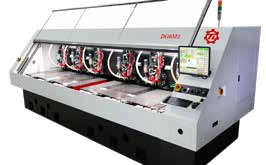
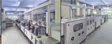
Machinery for PCB Manufacturing


Popular Services
PCBA Box Building
Acme delivers innovative ECMS solutions with advanced facilities, expert design, prototyping, and supply chain excellence.
LED Lighting
Arka pioneers advanced lighting solutions with precision, innovation, and ISO-certified excellence since its visionary inception.