Printed Circuit Boards (PCBs) are a crucial component of electronic devices, providing a platform for the placement and connection of electronic components. The PCB assembly process involves placing and soldering components onto the board. The quality of the PCB assembly process can have a significant impact on the overall performance and reliability of the device. In this blog post, we will discuss the top 10 mistakes to avoid in PCB assembly and provide best practices and guidelines for successful PCB manufacturing.
1. Poor Component Placement
Poor component placement can lead to problems such as electromagnetic interference, noise, and reduced signal integrity. To avoid this mistake, consider the placement of components on the board and follow these tips:
- Ensure proper spacing between components
- Group components according to function
- Follow recommended component placement guidelines
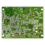
2. Inaccurate Footprint Design
Inaccurate footprint design can lead to problems such as poor connectivity, physical damage to components, and poor mechanical fit. To avoid this mistake, consider the footprint design and follow these tips:
- Verify component footprint accuracy before placement
- Use a library with verified footprints
- Consider the effects of manufacturing processes on footprint design
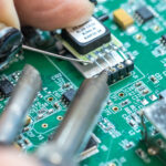
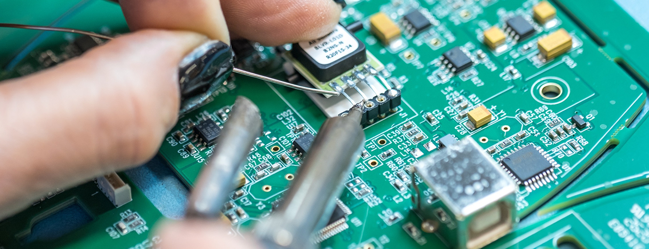
3. Poor Soldering Techniques
Poor soldering techniques can lead to problems such as weak connections, solder bridging, and cold solder joints. To avoid this mistake, consider the soldering techniques used and follow these tips:
- Use proper soldering tools and materials
- Follow recommended soldering techniques
- Inspect solder joints for quality and defects
4. Insufficient Trace Width and Spacing
Insufficient trace width and spacing can lead to problems such as signal loss, crosstalk, and electromagnetic interference. To avoid this mistake, consider the trace width and spacing and follow these tips:
- Follow recommended trace width and spacing guidelines
- Consider the effects of manufacturing processes on trace width and spacing
- Use simulation tools to verify trace width and spacing
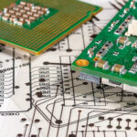
5: Poor PCB Design
A poorly designed PCB can lead to a range of issues during the assembly process and can result in a faulty final product. To avoid this mistake, ensure that the PCB design is optimized for the intended application, taking into consideration factors such as component placement, signal integrity, and thermal management.
ACME Circuit offers high-quality Printed Circuit Board Assembly services. Get reliable and efficient PCB assembly solutions for your electronic projects. Contact us now!